Silicon Solar Cell Design Reduces Thickness by 90%
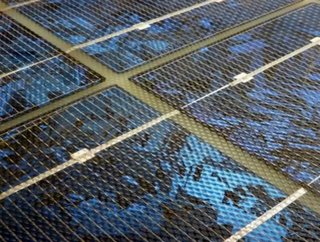
Engineers at MIT have discovered a new technique for building silicon solar cells that can trap rays of light as effectively as conventional silicon solar cells, while reducing the thickness by 90 percent. Using a pattern of tiny inverted pyramids etched into the surface of silicone, more light can be absorbed than solid silicon surfaces that are 30 times thicker.
A large bulk of the cost of solar arrays lies in the highly purified silicon—as much as 40 percent. Now, researchers are finding ways to make solar cells of the future more efficient, inexpensive and as thin and light as possible. Today, MIT engineers have brought us one step closer to the future of photovoltaics. Think of it as the iPhone of solar cells—the bulkiness, efficiency and accessibility of both technologies have certainly come a long way since the 80s.
SEE OTHER TOP STORIES IN THE ENERGY DIGITAL CONTENT NETWORK
Super-Sized Solar Power Plant Plans, San Luis Valley
Low Price Solar PV Racking Systems
Read more in June's issue of Energy Digital: Energy Turns to SPACE
The new findings are reported in the journal Nano Letters in a paper by MIT postdoc Anastassios Mavrokefalos, professor Gang Chen, and three other postdocs and graduate students, all of MIT’s Department of Mechanical Engineering.
According to Mavrokefalos, the method would enhance the efficiency of solar cells, no matter what the thickness.
Though other methods on the market have been employed to reduce cost of silicon, MIT's design would reduce the weight, which would also lead to savings in the installation process.
Using standard silicon-chip processing materials, the team reported that the indented pyramid texture is easy to fabricate. Two sets of overlapping laser beams used to create the dents are integrated into the silicon using lithography techniques. Potassium hydroxide is then used to burn parts of the surface not covered, and the crystal structure of the silicon sets the pyramid shape.

Thus far, the team has tested the surface of the silicon wafer. The next step will involve testing its efficiency as a photovoltaic cell comparable to traditional designs.
Supported under the US Department of Energy and the National Science Foundation, the project's potential impact is expected to be significant in providing an effective structure for photon management for enabling thin cells.